
You can’t fix what you can’t see.
As electronic devices become more compact, densely layered, and complex, traditional inspection methods are no longer enough. Internal defects in solder joints, vias, or semiconductor packaging can remain completely invisible, until they cause expensive failures in the field.
That’s where advanced X-ray inspection, and specifically inCiTe™ 3D X-ray Microscopy, comes in. With high-resolution 3D imaging, phase contrast, and nondestructive testing capability, inCiTe enables engineers and QA teams to find the flaws that others miss, before they become recalls.
In this article, we’ll answer frequently asked questions about electronics inspection, quality control, and failure analysis – and show how inCiTe is transforming inspection workflows with faster, deeper insight.
What is Electronics Inspection in Quality Control?
Electronics inspection in quality control ensures that electronic components, assemblies, and finished devices are meeting required performance, reliability, and safety standards.
With a thorough inspection process, electronics manufacturers are able to detect defects early, prevent product failures, and reduce production waste. Additionally, the inspection process is mandatory in electronics manufacturing.
Inspected electronic components include:
- Printed Circuit Boards (PCBs)
- Surface-Mount Technology (SMT) Assemblies
- Semiconductor Packages
- Connectors and Interconnects
- Sensors and Microelectromechanical Systems (MEMS)
- Batteries
What is the Difference Between Optical Inspection and X-ray Inspection?
Optical inspection – including both manual visual checks and Automated Optical Inspection (AOI) – is used to detect surface-level defects.
X-ray inspection, by contrast, allows inspectors to view internal and hidden structures. It uses X-ray imaging to penetrate through components and detect defects not visible on the surface.
While optical inspection is useful for identifying external scratches, misalignments, or missing parts, it falls short for inspecting:
- Microscopic features
- Multilayer PCBs
- Stacked packages
- Hidden solder joints
X-ray inspection overcomes these limitations, enabling a more thorough and dependable evaluation of electronic assemblies.
What Electronic Defects Can’t Be Seen Without an X-ray
X-ray inspection is essential to identify internal, hidden, or subsurface defects such as:
- Voids in BGAs (Ball Grid Arrays)
- Solder bridging between hidden pins
- Delamination inside PCB layers or semiconductor packages
- Via cracking in multilayer boards (e.g., barrel or corner cracks)
- Insufficient or excess solder under QFNs
- Misaligned or missing internal features
- Encapsulation voids in semiconductor packages
These defects are typically impossible to detect through visual inspection or even automated optical inspection (AOI), especially in high-density or multilayer designs.
How Often Are Electronics Inspected During Manufacturing?
Electronics are typically inspected multiple times throughout the manufacturing process to ensure quality. Inspection points vary by manufacturer, but the most common stages include:
- Pre-Production Inspection (PPI), which is conducted before mass production begins.
- During Production Inspection (DUPRO/Inline QA), which happens as products are being assembled.
- Pre-Shipment Inspection (PSI), which starts when production is finished but before products leave the factory.
- Unloading Inspections, which ensures products have been packaged correctly and were not damaged during transit.
- Failure analysis, which is conducted when a product has been flagged defective or is having performance issues.
What is Failure Analysis in Electronics Inspection?
Failure analysis, in the context of electronics inspection, is a forensic investigation to determine the root cause of an electronic device failure. A failure analysis is essential for correcting hidden issues in the manufacturer’s product design and/or production process.
While electronics inspection is essential throughout production, not all tools are built for every stage. This is where failure analysis comes into focus, and where inCiTe delivers its strongest value.
It’s not technically a routine inspection step, but can take place at any part of the production process when an issue has been flagged, whether in the early stages of production or after a product recall.
A failure analysis can be triggered:
- During production if a unit fails functional testing
- After a product has been deployed and returned under warranty
- As part of a root-cause investigation into intermittent performance issues
By precisely identifying the defect’s location and mechanism, manufacturers can:
- Correct design flaws or process issues
Improve long-term product reliability - Prevent future failures at scale
Unlike high-speed inline inspection tools, inCiTe’s high-resolution 3D imaging and phase contrast modes make it ideal for this investigative work. It allows engineers to see inside devices nondestructively, preserving the evidence while revealing defects in unmatched detail.
Why Do Electronics Manufacturers Need Non-Destructive Inspection Tools?
Electronic manufacturers rely on non-destructive inspection (NDI) tools, such as X-ray imaging, to avoid costly errors and protect product integrity without damaging the very components they need to inspect.
A single faulty batch can lead to:
- Significant financial losses in scrap, rework, or recalls
- Legal liabilities from regulatory non-compliance
- Brand damage if defective products reach the market
That’s why routine inspection must be non-destructive. Destroying a product to inspect it is impractical and wasteful, especially when many units may have no defects at all.
inCiTe solves this by enabling thorough, internal inspection without cutting, grinding, or opening the device. With phase contrast, 3D CT, and sub-micron resolution, it allows QA teams to:
- Detect hard-to-spot internal flaws
- Preserve the evidence for root-cause analysis
- Avoid unnecessary waste and delays
Destructive testing still has its place for detailed materials analysis or validation studies, but for most electronics inspection needs, NDI is faster, more efficient, and scalable.
What Should You Look for in Electronics X-ray Inspection Equipment?
Not all X-ray systems are created equal. When evaluating inspection tools for electronics, it’s important to consider how well the system can analyze dense SMT assemblies, multilayer PCBs, and complex semiconductor packages without compromising image quality or throughput.
Here are the key capabilities to look for:
High Resolution
High-resolution imaging can detect fine-pitch features, microvoids, cracked vias, thin solder joints, and miniscule structural defects. As components continue to shrink, resolution directly impacts how reliably you can assess solder integrity, interconnect quality, and overall assembly health.
inCiTe empowers QA teams to conduct deep investigations with fast, high-resolution scanning that captures what standard inspection tools can’t.
Phase Contrast Imaging
Traditional absorption-based X-ray struggles with low-density and low-contrast materials. Phase contrast enhances visibility by highlighting subtle differences in material thickness and composition. This can reveal issues such as delamination, resin-rich/poor zones, low-density inclusions, and internal material separation.
inCiTe is designed to enhance defect visibility, especially in areas where density differences are minimal but critical.
3D Capability (CT)
Two-dimensional X-ray provides only a projection, which can hide overlapping features. 3D imaging — via InCiTe’s Micro-CT system — offers depth information and cross-sectional views. This capability is essential for analyzing hidden joints (BGAs, QFNs, LGA packages), stacked dies, multilayer PCBs, embedded vias, and internal circuitry without actually cutting the board.
inCiTe’s Micro-CT system offers this full volumetric view, enabling nondestructive cross-sectioning without physical damage to the sample.
Compatibility With SMT Assemblies, PCBs, and Advanced Components
Modern electronics include diverse form factors and package styles. An inspection system should accommodate a wide range of board sizes, component heights, material densities, and package types. It should also integrate into failure analysis labs, engineering workflows, or offline QA processes with minimal setup.
InCiTe’s broad compatibility with SMT assemblies, PCBs, semiconductor components, and highly miniaturized electronics ensures it can handle the complexity of today’s designs.
How Does Electronics X-ray Inspection with InCiTe Work?
Electronics X-ray inspection with InCiTe combines advanced detector technology, multiple contrast modes, and an optimized workflow to give accurate insights into internal electronic structures. The system is designed to make complex inspection tasks (evaluating solder joints, PCB vias, wire bonds, connectors.etc) simpler and more reliable.
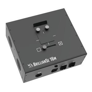
BrillianSe Detector Technology
At the core of InCiTe is its BrillianSe detector, a high-performance X-ray detector engineered specifically for high-resolution electronics inspection. It offers wide dynamic range for fine-detail, exceptional spatial resolution for microscopic components, and high sensitivity to shorten exposure times. The detector can reveal details normally invisible to conventional X-ray systems, enabling more confident inspection and failure analysis.
Phase Contrast + Absorption Contrast
InCiTe supports both absorption and phase contrast imaging to uncover a wider range of defects. Using both modes provides a more complete view of complex assemblies.
Absorption contrast highlights density differences, ideal for solder joints, vias, copper features, misalignments, and void detection.
Phase contrast improves the visualization of edges and low-density materials, revealing delamination, wire-bond integrity, polymer layers, adhesives, and micro-cracks.
Using both modes together gives engineers a more complete picture of internal structure and integrity.
Expanding What Users See
The BrillianSe detector enables:
- Sharp, high-definition images at both macro and micro scales
- Excellent visibility of subtle features and interfaces
- Real-time adjustments for fast repositioning and inspection
Workflow Simplicity
InCiTe streamlines the entire inspection process with:
- An intuitive interface and application-based presets
- Automatic optimization of exposure and contrast
- Quick sample loading and built-in measurement/reporting tools
Frequently Asked Questions about Electronics X-ray Inspection and inCiTe
Is inCiTe Suitable for Real-time Inspection?
inCiTe is best suited for failure analysis, not inline QA (quality checks within the production line).
The inCiTe 3D Microscope provides a highly detailed X-ray image and 3D reconstruction, which enables quality control teams to investigate and draw accurate conclusions about why an electronic component has failed. These insights are then used to pinpoint areas of improvement in the manufacturing process, helping prevent similar component failures in the future.
The specialized level of detail inCiTe provides is excellent in many use cases, but unnecessary for fast routine checks on the production and assembly line. Overall, the technology is better utilized in failure analysis.
Can X-ray inspection damage electronic components?
It’s not common, but yes, an X-ray inspection could damage electronic components. The X-rays’ energy and the radiation dosage needed for it can alter and/or damage components. QA teams need to be mindful of what X-ray inspection equipment they are using and whether there is a risk of damage.
The BrillianSe detector used in inCiTe is specifically optimized for fragile and miniaturized electronics. BrillianSe is specifically optimized for fragile components with heightened X-ray sensitivity (>50 keV) for quicker, high-clarity detection. This enables the detector to produce a comprehensive image without putting as much strain on the product being inspected.
By combining smart exposure control with detector sensitivity, inCiTe balances imaging performance and component safety, making it well-suited for inspecting advanced electronics without compromise.